
Infineon power density revolution
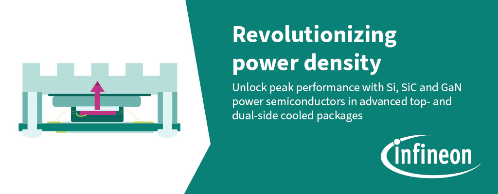
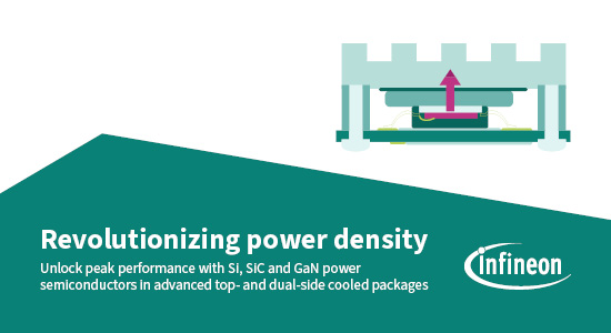
Unlock peak performance with Si, SiC and GaN power semiconductors in advanced top- and dual-side cooled packages
Unlocking the full potential of power electronics requires more than just the right switch. It demands the ideal synergy of power switch technology, topology, and thermal management. By combining Infineon's Si, SiC, and GaN technologies with advanced top- and dual-side cooling packages, engineers can push the boundaries of power density while maximizing efficiency and reducing costs.
Infineon as the leader in power systems, is mastering all three relevant semiconductor materials, with a broad portfolio of chip and package innovations in silicon (Si), silicon carbide (SiC) and gallium nitride (GaN). From low to high voltage including discrete, modules to fully integrated solutions, our full range of offering provides the precise tools needed to achieve peak performance and optimal price-performance in every design.
Key system benefits of top- and dual-side cooled power semiconductors
- Maximized power density:
Achieves higher power density by enabling component placement on both sides of standard PCBs. - Cost & assembly efficiency:
Simplifies the overall design and assembly process, resulting in significant cost reductions. - Superior thermal management:
Combines improved thermal resistance with best-in-class cooling performance for enhanced reliability. - Optimized electrical & material performance: Reduces stray inductance while utilizing cost-effective, standard FR4 PCB boards.
Choosing between Si, SiC and GaN: Which high-voltage power transistor is best for your application? | Watch the on-demand Webinar
Watch this on-demand webinar to understand the differences between Si, SiC, and GaN power transistor technologies, to learn how transistor packaging impacts performance and discover how application requirements drive technology selection.
The top-side cooled HDSOP package family and dual-side cooled package innovations
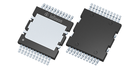
Infineon’s heat spreader dual small outline packages (HDSOP) family features a uniform 2.3 mm package height, enabling multiple discrete devices to be mounted on a single cold plate. This simplifies assembly, reduces design complexity, and enhances design flexibility. The package family is offered in top-side cooling (TSC) and bottom-side cooling (BSC) options. In addition, Infineon offers the DSO TSC and dual-side-cooled (DSC) package innovations.
PG-HDSOP-22
Q-DPAK
Innovative, top-side cooled SMD package, featuring CoolMOS™ and CoolSiC™ MOSFET.
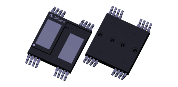
PG-HDSOP-16-2
Q-DPAK dual half-bridge
Features two CoolSiC™ MOSFET 1200 V G2 in top-side cooled Q-DPAK dual half-bridge package.
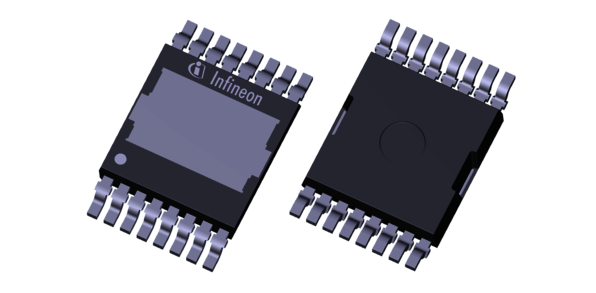
PG-HDSOP-16
TOLT
The transistor outline leadless top-side cooling package (TOLT) features Si, SiC and GaN technology.
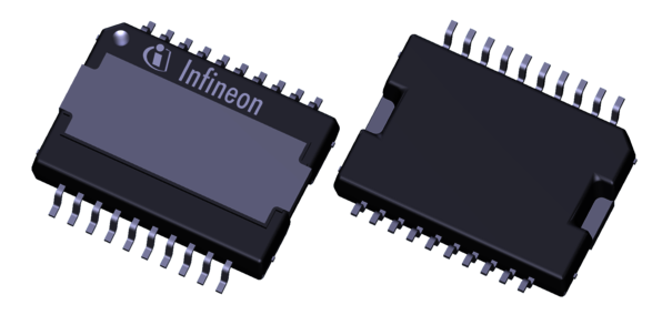
PG-DSO-20-90
DSO
The PG-DSO-20-90 top-side cooled package features the CoolGaN™ Transistors.
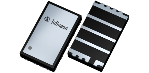
PG-TSON-6
PQFN 3x5
Dual-side cooled PQFN 3x5 SMD package featuring CoolGaN™ technology.
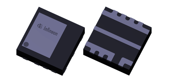
PG-TSON-4
PQFN 3x3
Dual-side cooled PQFN 3x3 SMD package featuring CoolGaN™ technology.
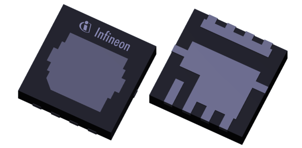
PG-WHSON-8
PQFN 3.3x3.3
Dual-side cooled PQFN 3.3x3.3 SMD package featuring OptiMOS™ technology.
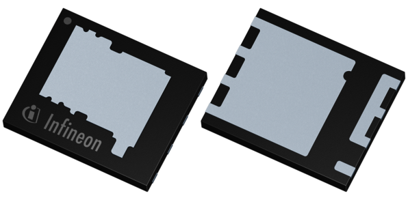
PG-WSON-8
SuperSO8 5x6
Dual-side cooled PQFN 3.3x3.3 SMD package featuring OptiMOS™ technology.
Explore the offering:
Silicon (Si) power semiconductors
Leading MOSFET solutions in advanced top- and dual-side cooled packages
Benefit from higher power density and system life with greater power dissipation thanks to the Q-DPAK and TOLT top-side cooled packages and innovative dual-side cooled package options. They provide a heat extraction through the top side of the component - thus only parasitic heat flux goes though the PCB. Higher power dissipation is therefore possible while the PCB runs cooler. The parasitic switching cell can now be routed optimally as the heat extraction no longer interferes with the distribution of current, allowing for faster commutation of larger currents.
With the broadest silicon power portfolio in the market, Infineon offers MOSFETs with unmatched quality, leading in all figures of merit (FOM) among silicon technologies - combining best price-performance with easy and robust to use solutions for every application across all voltage classes.
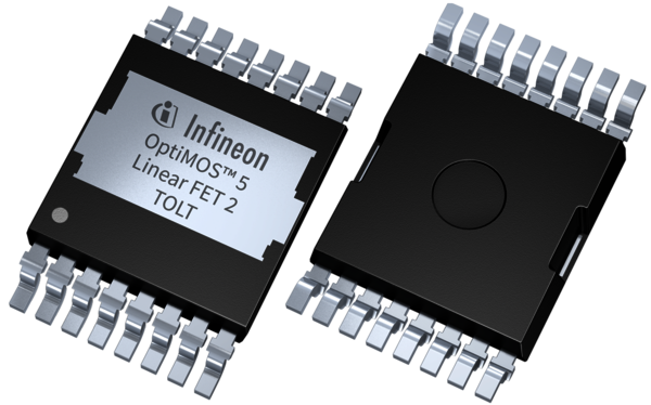
OptiMOS™ power MOSFETs 60 V – 200 V in TOLT package
Combining the leading-edge OptiMOS™ MOSFET technology with innovative TOLT package, these devices deliver best-in-class performance with ultra-low RDS(on), exceptional efficiency, and high power density—optimized for high-frequency switching applications.
IPTC007N06NM5
OptiMOS™ 5 power MOSFET
60 V
0.75 mΩ
IPTC011N08NM5
OptiMOS™ 5 power MOSFET
80 V
1.1 mΩ
IPTC017N10NM5LF2
OptiMOS™ 5 single
N-channel Linear FET 2
100 V
1.7 mΩ
IPTC014N10NM5
OptiMOS™ 5 power MOSFET
100 V
1.4 mΩ
IPTC025N15NM6
OptiMOS™ 6 power MOSFET
150 V
2.5 mΩ
IPTC068N20NM6
OptiMOS™ 6 power MOSFET
200 V
6.8 mΩ
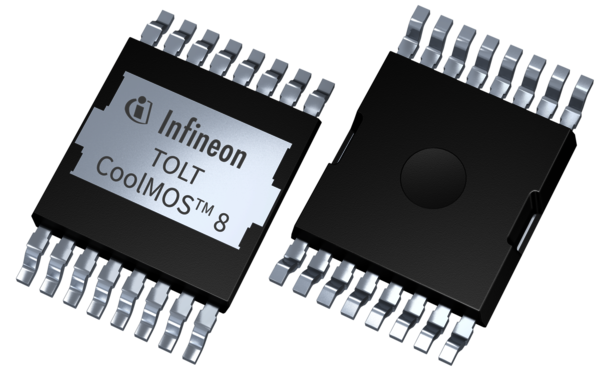
CoolMOS™ 8 Superjunction MOSFET in TOLT package
CoolMOS™ 8 in the compact TOLT package delivers industry-leading efficiency and power density. Its low-parasitic design ensures ultra-low losses for high-frequency, high-voltage applications.
IPLT60R024CM8
CoolMOS™ 8 SJ MOSFET
600 V
24 mΩ
IPLT60R037CM8
CoolMOS™ 8 SJ MOSFET
600 V
37 mΩ
IPLT60R055CM8
CoolMOS™ 8 SJ MOSFET
600 V
55 mΩ
IPLT60R070CM8
CoolMOS™ 8 SJ MOSFET
600 V
70 mΩ
IPLT60R099CM8
CoolMOS™ 8 SJ MOSFET
600 V
99 mΩ
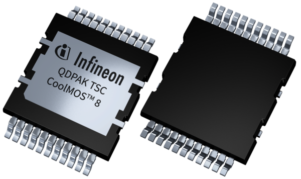
CoolMOS™ 8 Superjunction MOSFET in Q-DPAK package
The best-in-class RDS(on) of CoolMOS™ 8 enables customers to increase the power density level of their design, while the Q-DPAK top-side cooled packages allows to simplify the design and reduce assembly costs.
IPDQ60R007CM8
CoolMOS™ 8 SJ MOSFET
600 V
7 mΩ
IPDQ60R016CM8
CoolMOS™ 8 SJ MOSFET
600 V
16 mΩ
IPDQ60R024CM8
CoolMOS™ 8 SJ MOSFET
600 V
24 mΩ
IPDQ60R037CM8
CoolMOS™ 8 SJ MOSFET
600 V
37 mΩ
IPDQ65R008CM8
CoolMOS™ 8 SJ MOSFET
600 V
8 mΩ
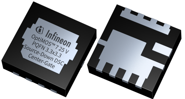
OptiMOS™ 5/6/7 in PQFN 3.3x3.3 Source-Down dual-side cooled package
The ultra-compact, dual-side cooled PQFN delivers exceptional thermal performance and power density. Its ultra-low RDS(on) and minimal switching losses enable highly efficient, high-frequency designs for space-constrained AC/DC, DC/DC, and motor drive applications.
IQE012N03LM5CGSC
OptiMOS™ 5 30 V
low-voltage
power MOSFET
1.15 mΩ
IQE020N04LM6CGSC
OptiMOS™ 6 40 V
low-voltage
power MOSFET
2.05 mΩ
IQE010N04LM7CGSC
OptiMOS™ 7 40 V
switching optimized
power MOSFET
1 mΩ
IQEH42NE2LM7ZCGSC
OptiMOS™ 7 25 V
switching optimized
power MOSFETs
0.42 mΩ
IQEH46NE2LM7UCGSC
OptiMOS™ 7 25 V
switching optimized
power MOSFETs
0.46 mΩ
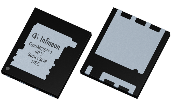
OptiMOS™ 7 in PQFN 5x6 Dual-Side Cooled package
With up to 3x wider SOA than OptiMOS™ 6 and 3.2 V threshold voltage, the OptiMOS 7 enables maximum reliability and reduced turn-on ruggedness. While the 70% lower trans-conductance improves current sharing, cuts voltage overshoot, and provides inherent short-circuit current limiting—ensuring robust performance under harsh conditions.
ISCH57N04NM7VSC
OptiMOS™ 7 40 V
motor-drives optimized
power MOSFETs
0.57 mΩ
ISCH75N04NM7VSC
OptiMOS™ 7 40 V
motor-drives optimized
power MOSFETs
0.75 mΩ
ISCH92N04NM7VSC
OptiMOS™ 7 40 V
motor-drives optimized
power MOSFETs
0.92 mΩ
Silicon Carbide (SiC) power semiconductors
400 V - 1200 V CoolSiC™ MOSFET in top-side cooled packages
Infineon’s CoolSiC™ MOSFET G2 leverages advanced SiC trench technology to deliver a major performance leap across AC/DC, DC/DC, and DC/AC systems. Compared to the previous generation, the G2 improves key figures-of-merit by over 20%, switching speeds by more than 30% and cuts power losses by 5–30% depending on load. The enhanced .XT interconnection boosts thermal capability by 12% and SMD power density by over 60%, enabling industry-leading on-resistance.
Built for extreme reliability, G2 specifies operation at 150°C, tolerates virtual junction temperatures up to 200°C, and offers rugged short-circuit and avalanche immunity, with field defect rates lower than mature silicon devices. Available in top-side cooled packages, it simplifies assembly, minimizes stray inductance, and reduces system costs, making it ideal for EV charging, PV inverters, energy storage, motor drives, Industrial SMPS and more.
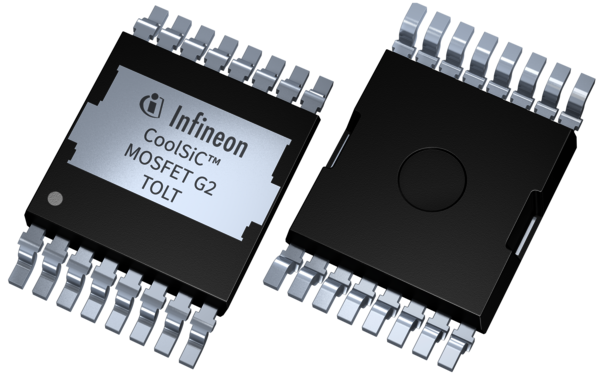
CoolSiC™ MOSFETs 400V and 650 V in TOLT package
The CoolSiC™ MOSFETs G2 in 400 V and 650 V combine cutting-edge Silicon Carbide technology with an innovative TOLT top-side cooled package to maximize system efficiency enabling ultra-compact and highly reliable designs.
IMLT40R011M2H
CoolSiC™ G2
400 V
11 mΩ
IMLT40R025M2H
CoolSiC™ G2
400 V
25 mΩ
IMLT40R045M2H
CoolSiC™ G2
450 V
45 mΩ
IMLT65R015M2H
CoolSiC™ G2
650 V
15 mΩ
IMLT65R033M2H
CoolSiC™ G2
650 V
33 mΩ
IMLT65R075M2H
CoolSiC™ G2
650 V
75 mΩ
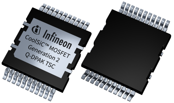
CoolSiC™ MOSFETs 650 V / 750 V / 1200 V in Q-DPAK package
Combine the high-performance CoolSiC™ G2 technology with the top-side cooled Q-DPAK package enables high power density, lower thermal resistance and reduced parasitisc inductance for compact, high-efficiency power systems.
IMDQ65R007M2H
CoolSiC™ G2
650 V
7 mΩ
IMDQ65R020M2H
CoolSiC™ G2
650 V
20 mΩ
IMDQ75R004M2H
CoolSiC™ G2
750 V
4 mΩ
IMDQ75R050M2H
CoolSiC™ G2
750 V
50 mΩ
IMCQ120R004M2H
CoolSiC™ G2
1200 V
4 mΩ
IMCQ120R026M2H
CoolSiC™ G2
1200 V
26 mΩ
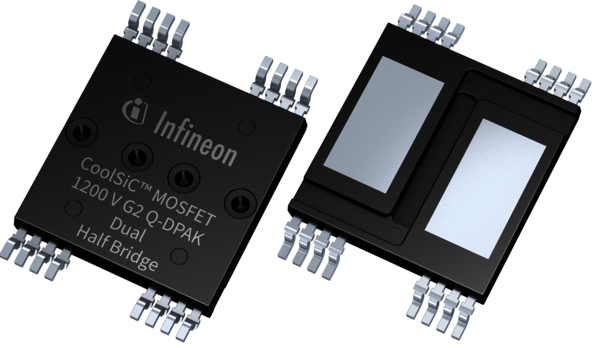
CoolSiC™ MOSFETs 1200 V in Q-DPAK dual half-bridge package
The Q-DPAK dual half-bridge integrates two 1200 V CoolSiC™ G2 MOSFETs in a compact dual half-bridge configuartion delivering superios thermal performance, higher power density, and simplified PCB layouts.
IMSQ120R012M2HH
CoolSiC™ G2
Half-bridge
1200 V
12 mΩ
IMSQ120R026M2HH
CoolSiC™ G2
Half-bridge
1200 V
26 mΩ
IMSQ120R040M2HH
CoolSiC™ G2
Half-bridge
1200 V
40 mΩ
IMSQ120R053M2HH
CoolSiC™ G2
Half-bridge
1200 V
53 mΩ
Gallium nitride (GaN) power semiconductors
CoolGaN™ Transistors in top- and dual-side cooled packages
Infineon’s CoolGaN™ Transistors redefine efficiency and power density for switch-mode power supplies, leveraging enhancement-mode GaN HEMT technology to deliver zero reverse recovery charge and ultra-low gate/output charge. This enables near-lossless, high-frequency switching that shrinks passive components and can double output power within the same footprint, achieving over 98% system efficiency. Rigorously qualified beyond industry standards through application-specific profiling and accelerated lifetime testing, CoolGaN™ ensures exceptional field reliability.
Complemented by Infineon’s EiceDRIVER™ gate driver ICs, the CoolGaN™ technology enables to achieve the best performance while minimizing costs, delivering significant BOM, CAPEX, and OPEX savings.
Available in dual side-cooled PQFN and top-side cooled DSO-20 and TOLT packages, CoolGaN™ maximizes system value across servers, hyperscale data centers, telecom, motor control, industrial solutions, residential solar and ESS, USB-C adapters, audio applications, and many more.
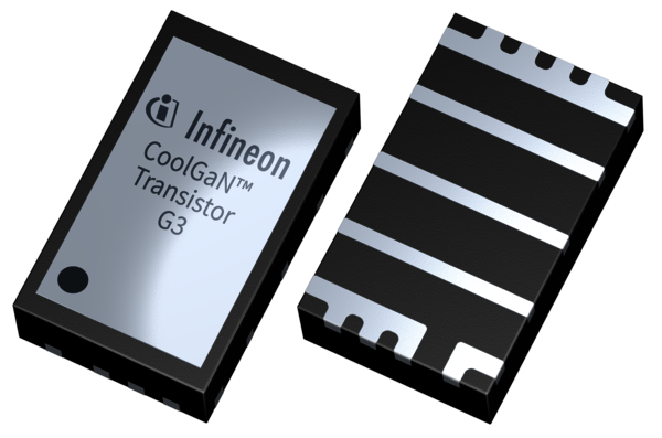
CoolGaN™ Transistors 60 V - 120 V in PQFN 3x5 package
The CoolGaN™ Transistor G3 in the dual-side cooled PQFN 3x5 package is a compact GaN solution that delivers ultra low on-resistance and high-frequency switching for space-constrained, high-efficiency power designs.
IGC019S06S1
CoolGaN™ G3
60 V
1.4 mΩ
IGC025S08S1
CoolGaN™ G3
80 V
1.8 mΩ
IGC033S10S1
CoolGaN™ G3
100 V
2.4 mΩ
IGC037S12S1
CoolGaN™ G3
120 V
2.4 mΩ
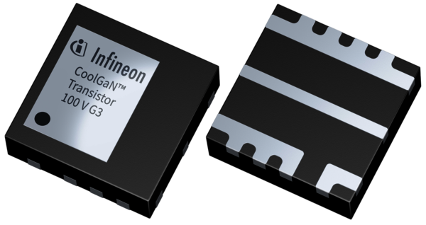
CoolGaN™ Transistor 100 V in PQFN 3x3 package
The CoolGaN™ Transistor 100 V G3 in the dual-side cooled PQFN 3x3 package is a compact normally-off e-mode GaN transistor available in 5 mΩ and 9.4 mΩ on-resistance options, enabling high power density designs.
IGB070S10S1
CoolGaN™ G3
100 V
5 mΩ
IGB110S10S1
CoolGaN™ G3
100 V
9.4 mΩ
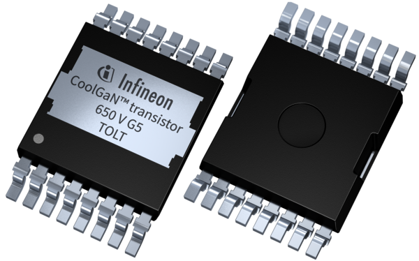
CoolGaN™ Transistor 650 V in TOLT package
The CoolGaN™ Transistor 650 V G5 in the top-side cooled TOLT package, is a high voltage GaN Transistor optimized for optimal power dissipation, allowing for increased efficiency at high-frequency operation enabling highly reliable designs.
IGLT65R110D2
CoolGaN™ G5
650 V
110 mΩ
IGLT65R055D2
CoolGaN™ G5>
650 V
55 mΩ
IGLT65R045D2
CoolGaN™ G5
650 V
45 mΩ
IGLT65R035D2
CoolGaN™ G5
650 V
35 mΩ
IGLT65R025D2
CoolGaN™ G5
650 V
25 mΩ
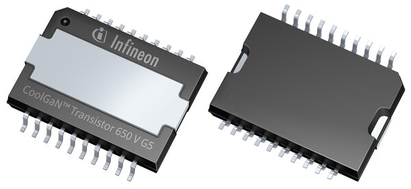
CoolGaN™ Transistor 650 V in DSO TSC package
The CoolGaN™ Transistor 650 V G5 in DSO TSC (PG-DSO-20) package is a high-voltage GaN transistor with the drain pad exposed on top, enabling direct heat transfer to a heatsink for best-in-class thermal performance.
IGOT65R025D2
CoolGaN™ G5
650 V
25 mΩ
IGOT65R035D2
CoolGaN™ G5
650 V
35 mΩ
IGOT65R045D2
CoolGaN™ G5
650 V
45 mΩ
IGOT65R055D2
CoolGaN™ G5
650 V
55 mΩ
Explore Infineon’s cutting-edge boards & designs
Just set up laboratory experiments or a first prototype with our evaluation boards, reference designs and demonstrators to evaluate our cutting-edge power semiconductor products.
Boards featuring OptiMOS™, CoolMOS™ and CoolSiC™
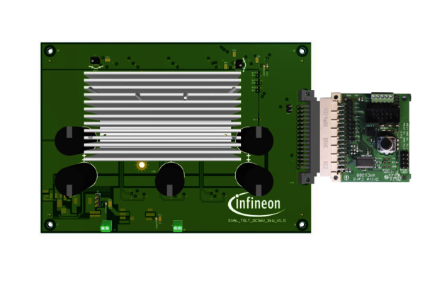
EVAL_TOLT_DC36V_2KW
2 kW BLDC motor drive inverter power board based on OptiMOS™ in TOLT with top-side cooling
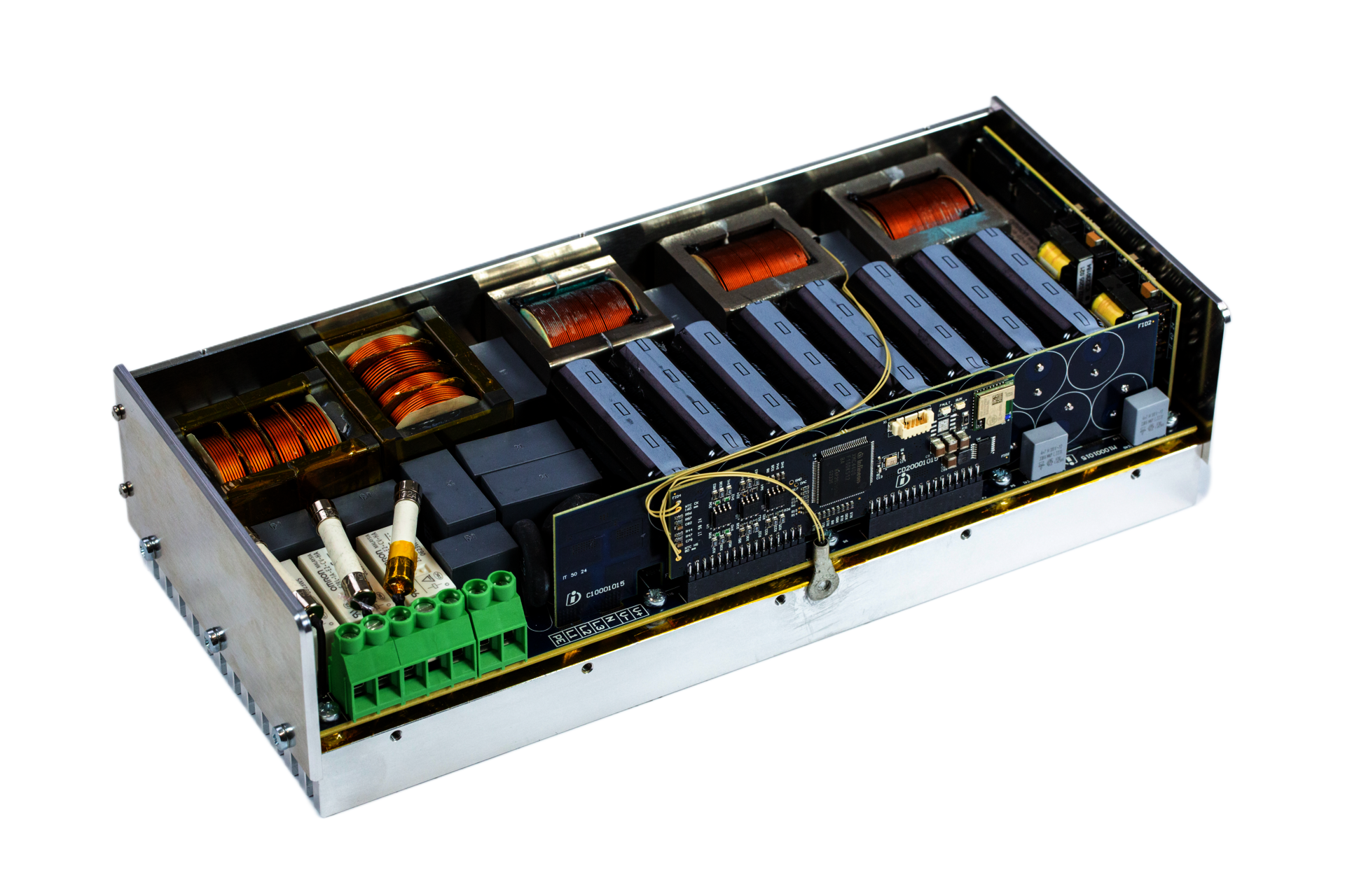
REF_11KW_PFC_SIC_QD
3L-ANPC bi-directional, top-side cooled converter for high efficiency (99.15% peak) and power density (>11kW/L) compatible with 3-ph and 1-ph grids
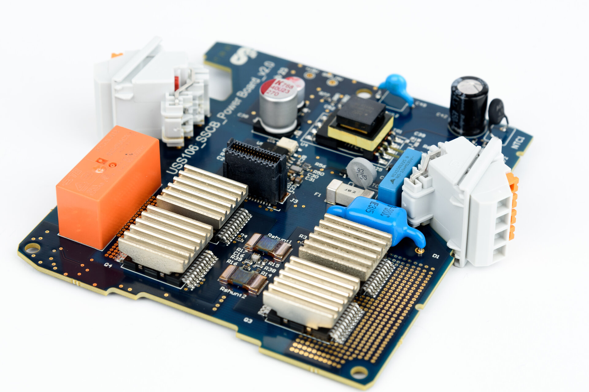
REF_SSCB_AC_DC_1PH_SIC
AC-DC solid state circuit breaker evaluation kit with interactive GUI, versatile topologies, and passive cooling
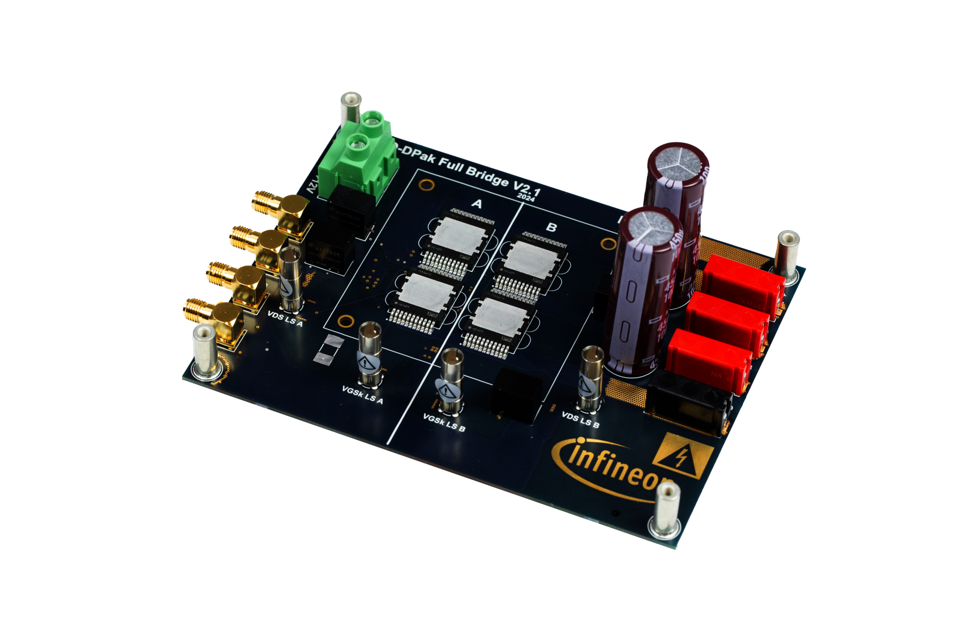
EVAL_QDPAK_FB_V2_1
Evaluation platform for high-speed switching of CoolSiC™ MOSFETs in Q-DPAK package in Full-Bridge topology
Boards featuring CoolGaN™
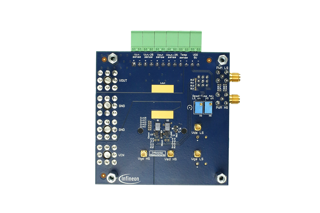
EVAL_7136U_100V_GANC
Half-bridge evaluation board with CoolGaN™ 100 V G3 and TDI EiceDRIVER™ 1EDN7136U
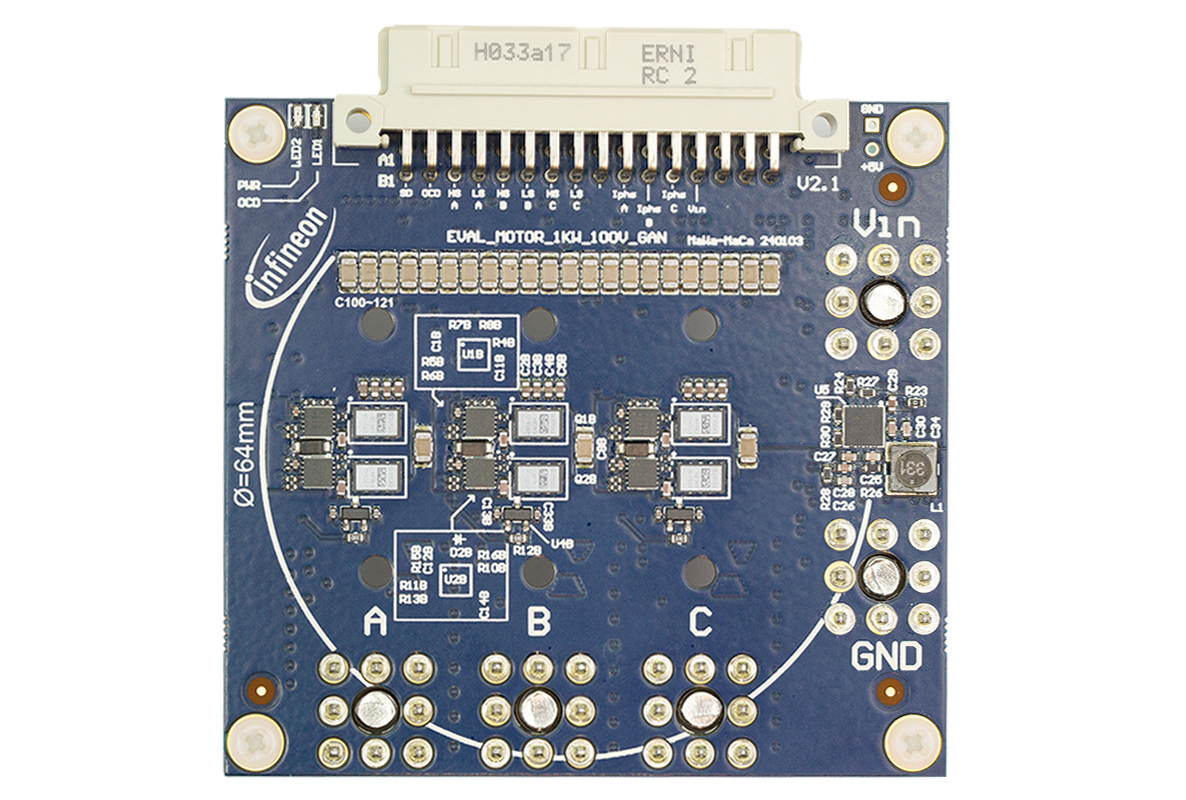
EVAL_MTR_48V20A_GAN
Evaluation board for low-voltage motor drive with CoolGaN™ Transistor 100 V G3
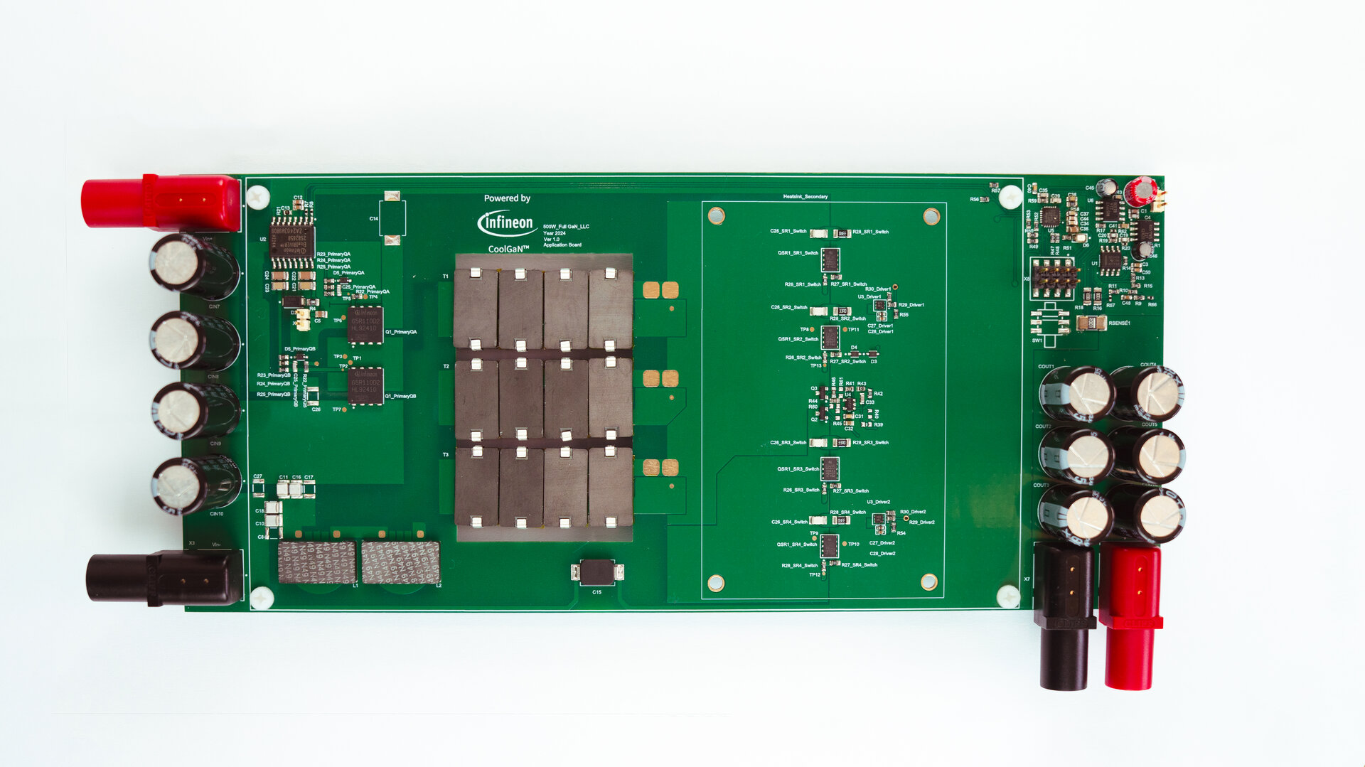
REF_LLC_500W_FULLGAN
500 W half-bridge full GaN LLC board for ultra-thin TV power supplies
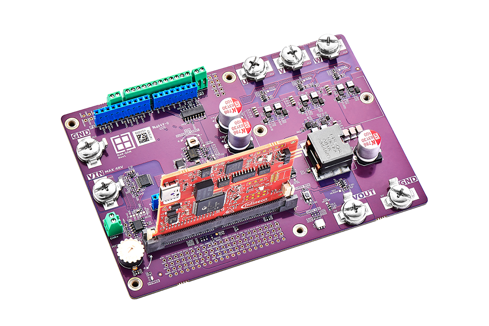
Rutronik Application Kit “RAK-GaN”
For motor control and power conversion, includes Infineon PSOC™ Control C3M5 Digital Power Control Card with PSOC™ C3 and CoolGaN™ 100 V G3 in the dual-side cooled PQFN 3x3 package.
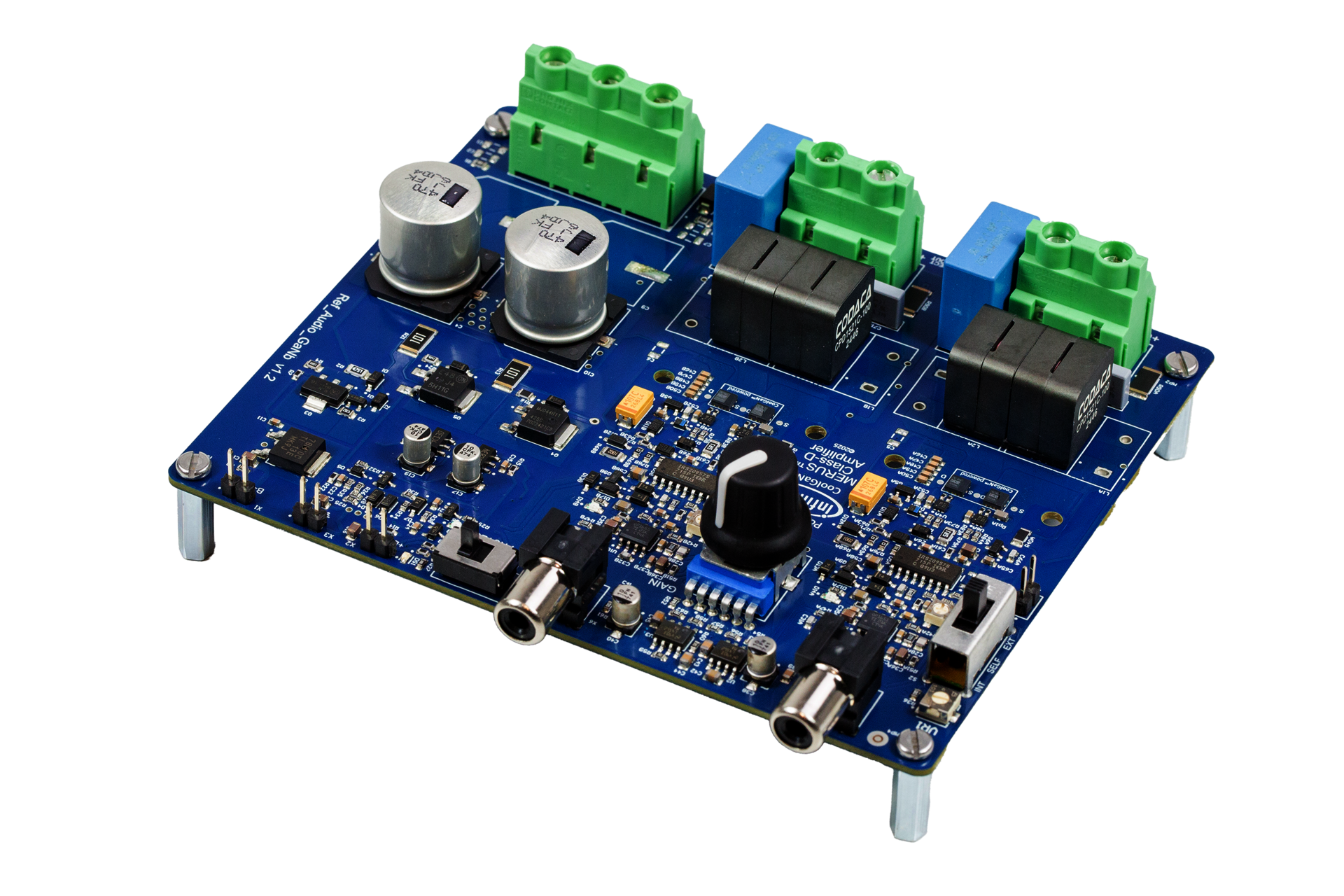
REF_AUDIO_GANB_750W
Class D audio evaluation board with CoolGaN™
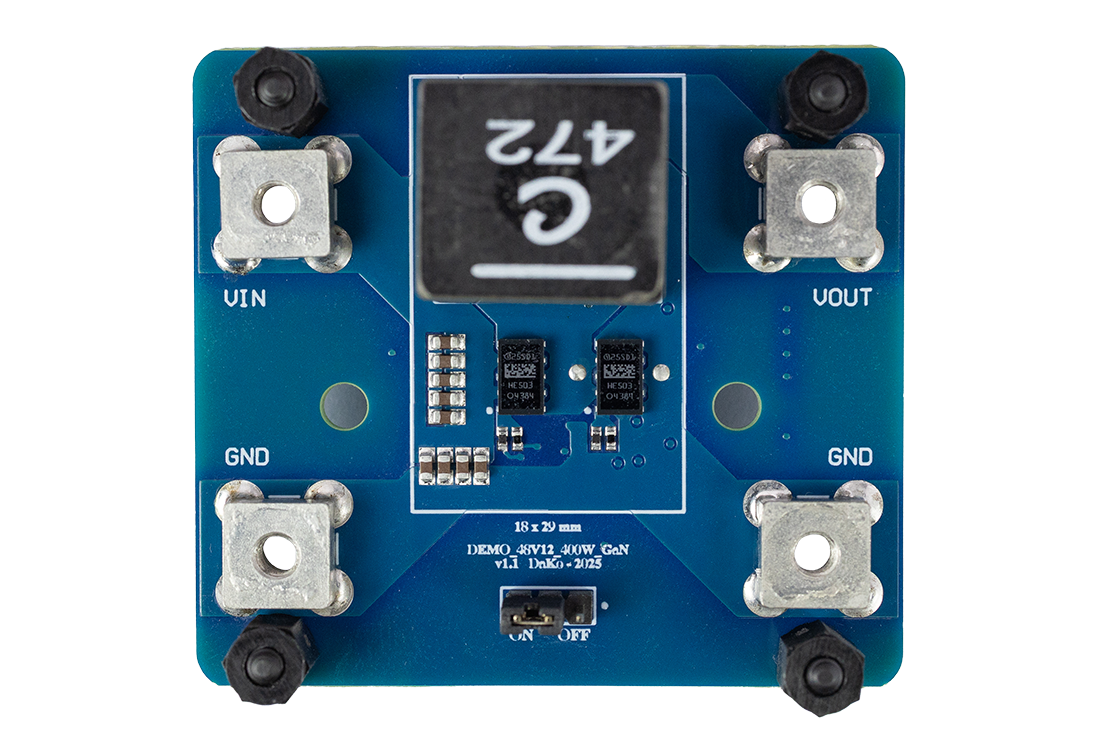
DEMO_48V12_400W_GAN
Non-isolated 400 W synchronous buck converter using CoolGaN™ 80 V G3
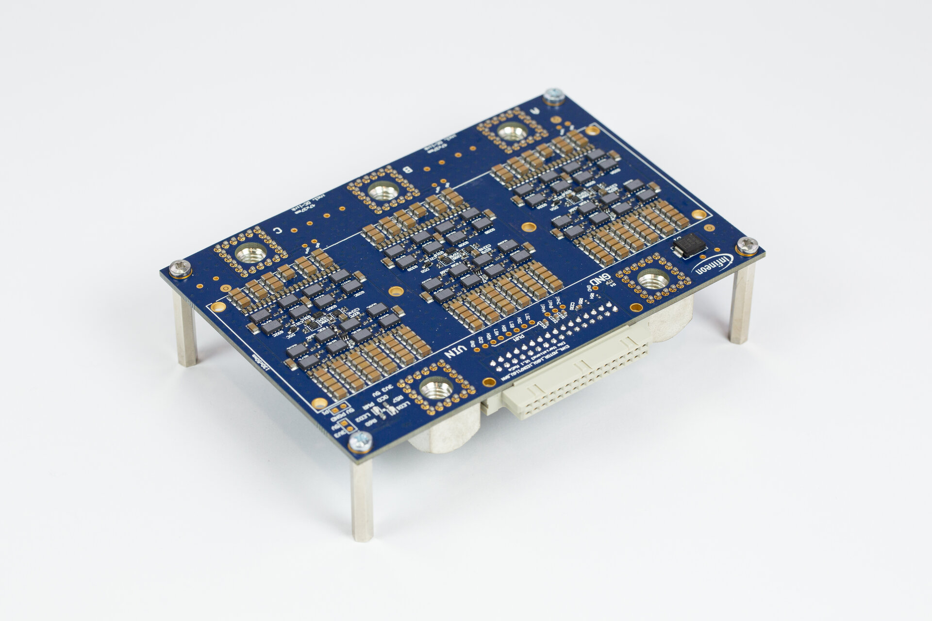
EVAL_MTR_48V150A_GAN
Evaluation board for low- and high-power motor drive solutions with CoolGaN™ 80 V G3
Featured Content
Whitepapers
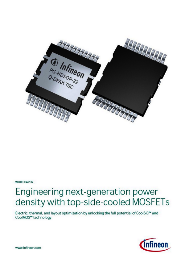
Engineering next-generation power density with top-side cooled MOSFETs
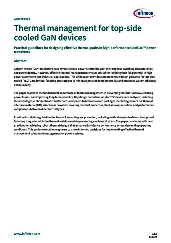
Thermal management for top-side cooled GaN devices - practical design guidelines
Application Notes
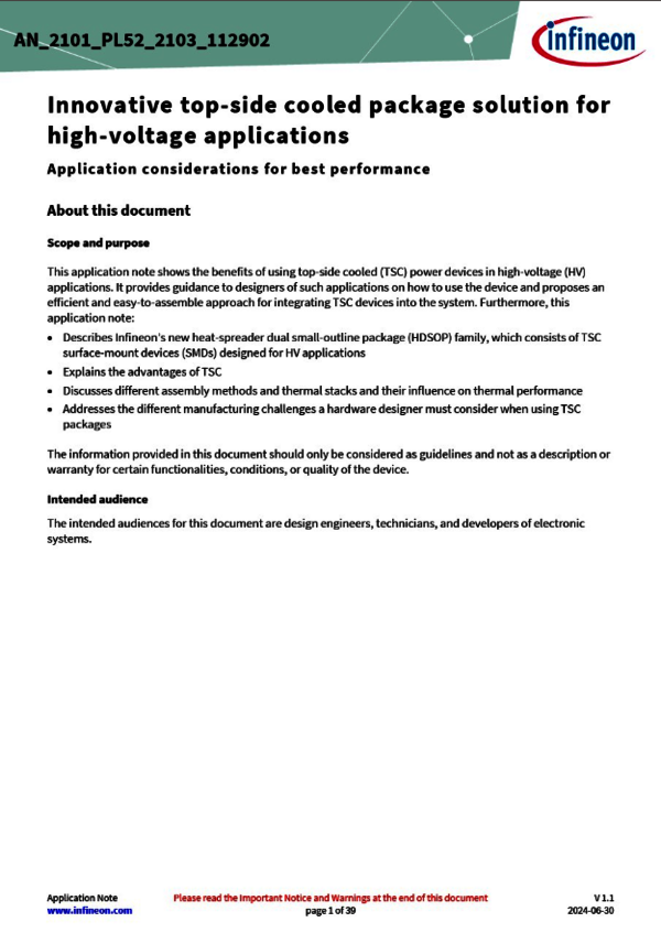
Innovative top-side cooled package solution for high-voltage applications
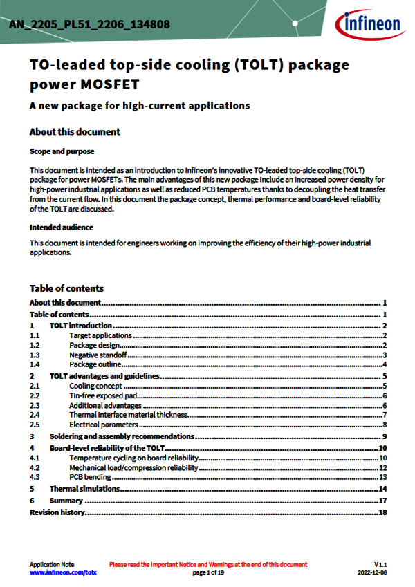
TO-leaded top-side cooled (TOLT) package power MOSFET
Selection Guides
Power system topology selection guide

Power and sensing selection guide 2026
Featured Videos

Discover a variety of trainings and online classes at the Infineon Academy Learning Platform, that will empower you with in-depth knowledge about Infineon's products, applications and more.