About Infineon Technologies
Semiconductors are crucial to solve the energy challenges of our time and shape the digital transformation. This is why Infineon is committed to actively driving decarbonization and digitalization. As a global semiconductor leader in power systems and IoT, we enable game-changing solutions for green and efficient energy, clean and safe mobility, as well as smart and secure IoT. We make life easier, safer, and greener. Together with our customers and partners. For a better tomorrow.
Infineon designs, develops, manufactures, and markets a broad range of semiconductors and semiconductor-based solutions, focusing on key markets in the automotive, industrial, and consumer sectors. Its products range from standard components to special components for digital, analog, and mixed-signal applications to customer-specific solutions together with the appropriate software.
Product range:
- Automotive: 32-bit automotive microcontrollers for powertrain, safety, driver assistance systems, infotainment and digital display systems; 3D ToF sensors; discrete power semiconductors; IGBT modules; industrial microcontrollers; magnetic and pressure sensors; memory ICs (NOR Flash, SRAM, nvSRAM, F-RAM); power ICs; radar sensor ICs (77 GHz); SiC diodes, SiC MOSFETs and SiC modules; transceivers (CAN, CAN FD, LIN, Ethernet, FlexRay™); voltage regulators
- Green Industrial Power: bare die business; discrete IGBTs; Driver ICs; IGBT modules (low-power, medium-power, high-power); IGBT module solutions including IGBT stacks; intelligent IGBT modules with integrated control unit, driver and switch; SiC diodes, SiC MOSFETs, SiC modules
- Power & Sensor Systems: 3D ToF sensors; chips for gas sensors; chips for MEMS microphones; chips for pressure sensors; control ICs for power switches; customized chips (ASICs); discrete low-voltage, mid-voltage and high-voltage power MOSFETs (Si-based); GaN power switches; GPS low-noise amplifier; low-voltage and high-voltage driver ICs; radar sensor ICs (24 GHz, 60 GHz); RF antenna switches; RF power transistors; SiC diodes, SiC MOSFETs; TVS (transient voltage suppressor) diode; USB controller
- Connected Secure Systems: connectivity solutions (Wi-Fi, Bluetooth, BLE); embedded security controllers; microcontroller for consumer electronics and industrial applications; security controllers (contact-based, contactless, dual-interface)
Featured Products and Applications
Energy Efficiency
- Power generation from renewable energy sources: IGBT modules, SiC modules, discrete power devices
- Energy transmission and distribution: High-power IGBT modules
- Energy storage: IGBT modules, SiC modules
- Energy usage: Discrete power devices, IGBT modules, driver ICs, MCUs, SiC modules, SiC MOSFETs, SiC diodes, GaN HEMTs
Mobility
- Electro-mobility: IGBT modules, SiC modules, discrete power devices, MCUs, sensors
- Charging infrastructure for electro mobility: IGBT modules, SiC modules, SiC discretes, discrete power devices, MCUs, security solutions
- Automated driving: Sensors, radar, MCUs, power devices, memories, connectivity and security solutions
- Passenger and freight transport: High-power IGBT modules
- Infotainment: MCUs, touch control, Wi-Fi/BT controllers, USB Type-C PD controllers
Security
- Mobile devices: Security solutions based on contactless and dual-interface security controllers
- Authentication for the IoT: Embedded security solutions
- Industrial application: Embedded security solutions, TPMs, connectivity solutions
- Connected vehicles: Embedded SIMs, connectivity solutions
- Integrity of devices: TPMs
IoT and Big Data
- Smart cars: Sensors, radar, MCUs, power devices, memories, connectivity solutions, security solutions
- Smart home and smart building: Sensors, MCUs, power devices, memories, connectivity solutions, security solutions
- Smart things: Sensors, MCUs, power devices, memories, connectivity solutions, security solutions
- Smart factory: Sensors, MCUs, power devices, memories, connectivity solutions, security solutions
- Data and communication infrastructure: Power devices, memories, SiC devices, GaN HEMTs, RF devices
New Products Introduction
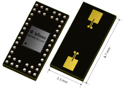
BGT60LTR11AIP -completely autonomous radar sensor
The BGT60LTR11AIP MMIC is a fully integrated microwave motion sensor including Antennas in Package (AIP) as well as built-in motion and direction of motion detectors. A state machine enables operation of the device autonomously, i.e., without an external microcontroller or further signal processing. The detection threshold or sensitivity has 16 different levels in order to fulfill a configurable detection range from 0.5 m up to 7 m with a typical human target Radar Cross Section (RCS).The device can achieve power consumption of less than 2mW with adjustable duty cycling.
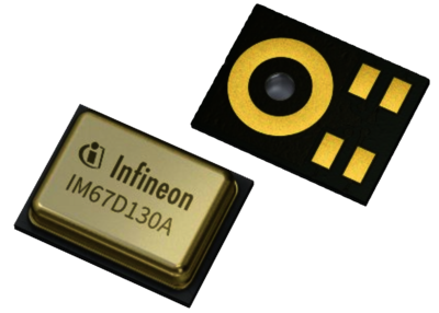
XENSIV™ –IM67D130A high performance MEMS microphone for automotive applications
XENSIV™ -IM67D130A high performance MEMS microphone for automotive applications. Our high performance digital MEMS microphones are suited to all applications inside and outside the car, where the best audio per-formance in harsh automotive environments is required. These automotive microphones enable distortion-free audio capturing for all speech-related applications improving speech intelligibility for voice recognition algorithms. In addition, they perfectly support acoustic noise cancellation with its flat frequency and stable phase response. Other highlights include close sensitivity and phase matching, making automotive XENSIV™ MEMS microphones ideal for beamforming arrays.We offer two derivatives:IM67D130A high performance digital MEMS microphone IM67D120A high performance digital MEMS microphone for 16-bit codes.
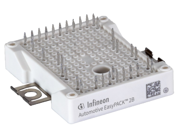
EasyPACK™ Automotive IGBT 750V Half Bridge -FF300R08W2P2_B11A
The EasyPACK™ 2B is a very compact and flexible halfbridge solution, optimized for inverter applicationsof hybrid and electric vehicles up to 230Arms. The module uses the benchmark EDT2 IGBT generation allowing 750V blocking voltage and IcN of 300A. The chipset has benchmark current density combined with short circuit ruggedness for reliable inverter operation under harsh environmental conditions. The EDT2 IGBTs also show excellent light load power losses, which helps to improve system efficiency over a real driving cycle. The EasyPACK™ package is fully qualified for automotive applications and is validated according to AQG 324. Its high power cycling capability as well as the high creepage and clearance distances add to the product reliability. The power module comes with PressFIT Pins for the signal terminals to avoid additional time consuming selective solder processes, which provides cost savings on system level and increases system reliability.
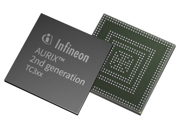
32-bit TriCore™ AURIX™ TC3Ex family
32-bit TriCore™ AURIX™ TC3Ex family. Infineon releases its AURIX™ TC3Ex microcontroller family. It comes back with an increase in performance, memory sizes, con-nectivity and more scalability to address the new automotive trends and challenges. In terms of performance, T3Ex offers 4 cores running at 300 MHz and up to 1.5 MBytes embedded RAM, and consuming below 2 W. Its mirrored embedded flash banks offers A/B swap capabilities.
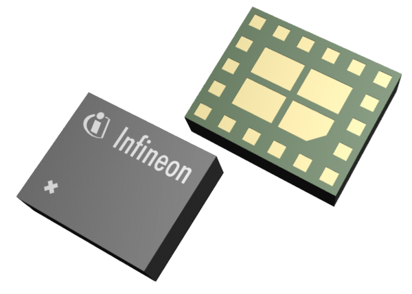
BGSX44MU18 -4P4T MIPI antenna cross switch
BGSX44MU18 -4P4T MIPI antenna cross switch The BGSX44MU18 RF CMOS switch is specifically designed for LTE and 5G FR1 four-antenna applications. This 4P4T cross-switch offerslow insertion loss and low harmonic generation. The switch is controlled via aMIPI RFFE control interface. The on-chip controller allows power-supply voltages from 1.65 to1.95 V. The switch features direct-connect-to-battery functionality and DC-free RF ports. Unlike GaAs technology, external DC blocking capacitors at the RF ports are only required if DC voltage is applied externally. The device has a very small size of only 2.0 mm x 2.4 mm and a thickness of 0.63 mm.
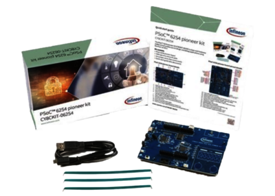
PSoC™ 62S4 Pioneer Kit (CY8CKIT-062S4)
The PSoC™ 62S4 Pioneer Kit features the PSoC 62 MCU CY8C62x4 (CY8C6244LQI-S4D92) with: 150-MHz Arm® Cortex®-M4 and 100-MHz Arm Cortex-M0+ cores, 256KB of Flash, 128KB of SRAM, programmable analog blocks including two 12-bit SAR ADCs, programmable digital blocks, Full-Speed USB, a serial memory interface, a CAN-FD interface, and industry-leading capacitive-sensing with CAPSENSE™.
NPI Download
See the latest products in our shop


