
Battery Formation: Your Critical Bottleneck?
Infineon Answers with More Accuracy, Higher Power Density, and Greater Efficiency
The world witnesses a rapid rise in the number of battery powered devices - among them more and more electric vehicles (EVs). Consequently, battery manufacturers see themselves confronted with a steady growing demand and hence with the challenge to increase efficiency throughout their factories. Also in battery formation - the known bottleneck given the big investment and the extremely time consuming process. We at Infineon know the market and we understand the requirements industry players have. Our today's sense for innovation will be your competitive advantage of tomorrow. Continue reading and find out about our full-spectrum system solutions with the respective highlight products.
Battery Formation (Last Step in the Production Process, Vital for Market Readiness)
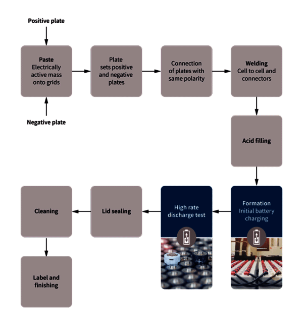
Battery production: 8 main steps
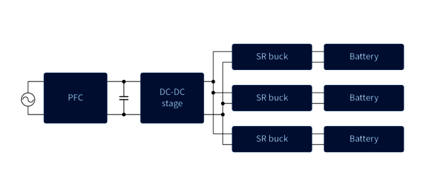
Block Diagram of Battery Formation System
Battery formation is the last step of producing a battery. More precisely, formation is the initial charge and discharge of a newly produced battery. The process, for which high voltage and current accuracy are critical, relies on special battery formation equipment. Formation cycling is expensive because it takes considerable time (up to 20 hours) as each cell must be monitored separately. A true bottleneck!
Additionally, with 29 percent the task of "formation cycling and testing" currently accounts for the biggest portion in the breakdown of installed capital equipment costs for the baseline plant.
Prerequisite for market readiness
The process which activates the material in a newly assembled battery cell or pack is essential as it heavily impacts a battery's quality and cost. Also ensuring that it lasts for the indicated lifetime. Only after testing a battery it can be deemed market-ready.
Power System Solutions (Making the Equipment More Accurate and Efficient)
Success factors:
Ideally, a suitable battery formation power system solution
- Enables high voltage and current accuracy up to 0.01%
- Provides thermal management of MOSFETs for higher current rating requirements
- Increases the overall power density with higher current rating size
- Improves the reliability in 24/7 operation cycles
In general, manufacturers prefer a quality system solution that is not over-engineered. It should have an attractive cost-performance ratio, yet be reliable and stable to facilitate continuous operation under the given conditions. High power density helps them to decrease the solution’s size. And when opting for a standard platform - scalable to fit a wide range of requirements - they are even able to reduce their time to market.
Infineon’s full-spectrum system solutions
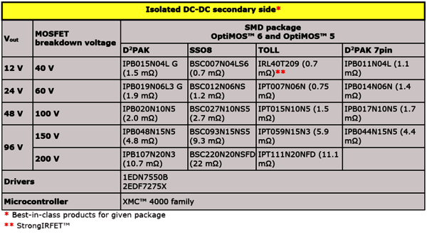
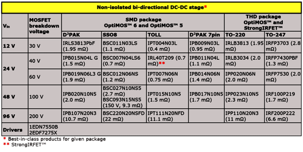
Infineon empowers successful designs with more accuracy, higher power density, and greater efficiency. Our full-spectrum system solutions range from the AC grid to battery which requests a highly efficient and power-dense PFC stage and an isolated DC-DC stage. A totem pole PFC converter and a bi-directional DC-DC converter are recommended in our full system silicon solution. An enormous design flexibility will allow designers to meet varying requirements.
Particularly noteworthy: for the non-isolated DC-DC buck-boost stages our products enable the achievement of high power density leading to improved efficiency. Infineon's comprehensive portfolio of surface mounted devices (SMD) will satisfy those prioritizing lower BOM count and higher power density compared with a package supported by the PCB board.
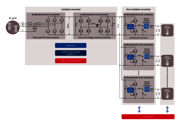
System Diagram: Bi-directional Battery Formation
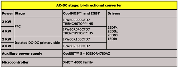
AC-DC Stage: Bi-directional Converter
Isolated DC-DC Secondary Side
Non-isolated Bi-directional DC-DC Stage
Highlight Products (Recommended MOSFETs and Driver ICs)
MOSFETs:

BSC011N03LSATMA1
Transitional MOSFET, 30 V, PG-TDSON-8
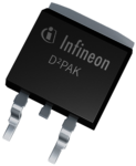
IPB009N03LGATMA1
Transitional MOSFET, 30 V, PG-TO263-7,
D²PAK 7pin
IPT004N03LATMA1
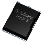
Differentiated MOSFET, 30 V, PG-HSOF-8
IRLS3813PBF
Single N-channel HEXFET® Power MOSFET, 30 V, D2PAK

BSC007N04LS6ATMA1
OptiMOS™ 6, differentiated MOSFET, 40 V,
PG-TDSON-8

IPB011N04LGATMA1
Transitional MOSFET, 40 V, PG-TO263-7,
D²PAK 7pin
IRL40T209ATMA1
StrongIRFET™, 40 V, PG-HSOF-8
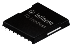
BSC012N06NSATMA1
Differentiated MOSFET, 60 V, PG-TSON-8

IPB019N06L3GATMA1
OptiMOS™ 3, Transitional MOSFET, 60 V,
PG-TO263-3

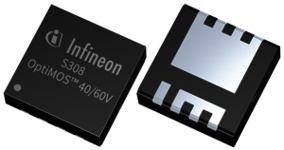
IPT007N06NATMA1
OptiMOS™, Differentiated MOSFET, 60 V,
PG-HSOF-8

BSC027N10NS5ATMA1
Differentiated MOSFET, 100 V, PG-TSON-8

IPB017N10N5ATMA1
OptiMOS™ 5, Differentiated MOSFET, 100 V, PG-TO263-7,
D²PAK 7pin
IPB020N10N5ATMA1
OptiMOS™ 5, Differentiated MOSFET, 100 V,
PG-TO263-3
IPT015N10N5ATMA1
OptiMOS™ 5, Differentiated MOSFET, 100 V,
PG-HSOF-8
BSC093N15NS5ATMA1
Differentiated MOSFET, 150 V, PG-TDSON-8
BSC220N20NSFDATMA1
OptiMOS™ 3, 200 V, TSON-8-3

IPT111N20NFDATMA1
OptiMOS™ 3, Differentiated MOSFET, 200 V,
PG-HSOF-8

IPW60R105CFD7XKSA1
CoolMOS™ CFD7, high power MOSFET, 600 V,
PG-TO247-3
IPW60R090CFD7XKSA1
CoolMOS™ CFD7, high power MOSFET, 600 V,
PG-TO247-3
IPW60R040CFD7XKSA1
CoolMOS™ CFD7, high power MOSFET, 600 V,
PG-TO247-3
DRIVER ICs:
1EDN7550BXTSA1
Single-channel EiceDRIVER™, truly differential inputs, PG-SOT23-6
2EDF7275FXUMA1
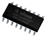
EiceDRIVER™ 2EDi family, dual-channel, functional isolated, PG-DSO-16
2EDF7275KXUMA1
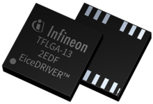
EiceDRIVER™ 2EDi family, dual-channel, functional isolated, PG-TFLGA-13
Recommended Evaluation Board (Enabling Thorough Testing and Evaluation)
Image
Board Name and Key Components
Description and Target Applications
Key Features and Benefits
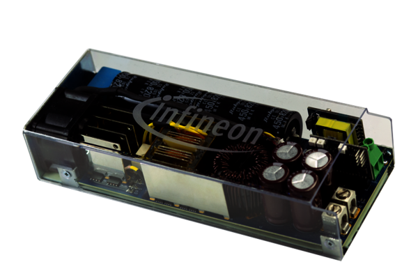
EVAL_3K3W_BIDI_PSFB
3300 W, 54 V bi-directional SMPS phase-shift full-bridge solution featuring 600 V CoolMOS™ CFD7 and XMC™
Infineon Components:
- 600 V CoolMOS™ CFD7 Superjunction MOSFET (IPL60R075CFD7)
- 150 V OptiMOS™ 5 power MOSFET in Super SO-8 package (BSC093N15NS5)
- Safety isolated gate driver EiceDRIVER™ (2EDS8265H)
- Functional isolated gate driver EiceDRIVER™ (2EDF7275F)
- XMC4200 microcontroller for control implementation
(XMC4200-F64k256BA) - Quasi-resonant flyback PWM controller (ICE5QSAG) with external 800 V CoolMOS™ Superjunction MOSFET (IPU80R4K5P7)
- CoolSiC™ Schottky diode 650 V G6 (IDH08G65C6)
- Medium power AF Schottky diode (BAT165)
- DC-DC step-down voltage regulator (IFX91041EJV33)
This evaluation board represents a complete system solution for a
3300 W telecom/battery charging DC-DC converter block which achieves 98% efficiency peak. The DC-DC converter is composed of a ZVS PSFB with bi-directional capability (patent pending).
Target Applications: battery formation power system, EV charging, telecom
Features:
- Innovative cooling concept and stacked magnetic structure for high power density in a full SMD solution
- Full digital control. Peak current mode and novel control algorithms (patent pending) enabling best voltage class devices and improved performance
- Bi-directional capability of PSFB without additional circuitry or impact on forward operation performance (patent pending)
- High efficiency PSFB design at the level of fully resonant topologies (LLC)
- Fast body diode devices for improved reliability in all working conditions
- Graphical user interface (GUI available for customers upon registration)
Benefits:
- Optimal use of CoolMOS™ and OptiMOS™ best-in-class devices
- Full SMD solution. Reduced BOM and assembly effort
- High efficiency converter block realized by a low complexity topology