Highly complex “smart” applications - audio processing, face recognition, gateway, etc. – therefore require high-performance MPU series such as RZ/A and RZ/G. Not only the high level of performance is particularly pleasing: Each series provides a 2D (RZ/A) or 3D graphics controller (RZ/G) and accelerator that supports two high-resolution video channels.
The RZ/A and RZ/G families deliver the ability to incorporate an additional DRAM for data storage. Moreover, the MPU of the RZ/A1 series has an integrated on-chip memory of up to 10 MB SRAM – unlike processors from other suppliers that work exclusively with external RAM and flash. Code and data (including graphical data) can be executed or read directly from the large SRAM or from the external QSPI memory via XIP. It is also noteworthy that the QSPI flash can run in DDR mode, thereby doubling the speed of the NOR flash. The EMI problem between MPU and DRAM is eliminated and fewer PCB layers are required. In addition, the popular QFP package can be used. These factors help to reduce production and development costs significantly. Thanks to the size of the internal memory, developers do not require further power management ICs. RZ/A1LC, RZ/A1L, and RZ/A1lU also offer a SDRAM interface in case the customer needs more RAM. The RZ/A is therefore well suited for development engineers who need a powerful MPU, want to switch from an MCU to an MPU while avoiding the drawbacks of an MPU design.
Concentrated graphics power
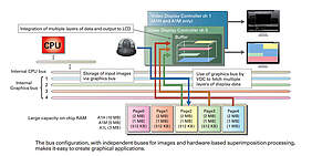
Thanks to the four dedicated internal graphics buses (AXI), each boasting a width of 32 bits, the RZ/A offers enormous graphics performance. Seeing as the internal SRAM can be used as a frame buffer (with up to 10.64 Gbps), the video controller can retrieve the image faster than with an external DRAM solution. The RZ/A supports two independent LCD displays with a resolution of 1280x800 and up to two CMOS camera inputs.
Hardware-accelerated 2D vector graphics (OpenVG) can be used to create a more attractive graphical user interface that is not distorted by image magnification. Processing is thus outsourced from the core to the GPU (graphic processing unit), so that the MPU core can execute more important algorithms. OpenVG is suitable for accelerating flash memories and scalable vector graphics.
Image 1: The bus configuration, with independent buses for images and hardware-based superimposition processing, makes it easy to create graphical applications.
If you are planning an application that requires certain graphic properties, Renesas offers three tools to choose from: DISPLAY IT!, STREAM IT!, and the GENMAI CPU board. Hardware reference designs (plans and layout) and demos are also available.
Software – simple, comfortable, powerful
The RZ/A is an easy-to-use MPU product for developers who want high performance without having to acquire full, detailed Linux knowledge. Thanks to the Renesas ecosystem and the corresponding community, developers can focus more on the application layer. Two operating system types can run on the RZ/A: RTOS or Embedded Linux.
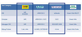
RTOS provides customers with four types of development environment: Renesas e²Studio, IAR, ARM DS-5, and Green Hills Multi.
Image 2: Four available IDEs, compiler, and debugger
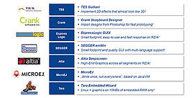
The software stacks with file system, USB stack, and network stack for each RTOS can be selected from Express Logic, Segger, and Micrium. Many different third-party GUI frameworks - Tes Guiliani (based on FreeRTOS, free because it is licensed by Renesas), Crank, Segger, Tara, Altia, and Draupner - can also speed up development work. Tes Guiliani is suitable for highly qualified GUI applications and the 2D effects reach an optical level close to 3D. The mass production license for Tes Guiliani is also based on the license for FreeRTOS and is therefore free of charge.
Box: Rutronik offers a system solution with RZ/A1H and Tianma TFT screen with Segger emWin. The kit is immediately available from stock.
Image 3: Available GUI frameworks for RZ/A
As when carrying out development work with traditional embedded Linux, the developer can use LTS Ubuntu Linux as the host. Renesas offers a BSP porting guide and a tool to help create the BSP when the customer is developing their own board. Additionally, uboot is available on the GitHub platform in order to initially configure a certain part of the board and to start Linux. With the help of buildroot, a cross-compilation toolchain, bootloader, kernel, and image of the root file system can be created. This makes actual application, understanding, and changes much easier. Two different Linux images (Linux 4.9 and 4.14) are available on GitHub for this purpose.
No performance without a memory
However, performance alone is not enough – even with RZ/A and RZ/G, nothing works without a program memory. Additional external flash is required to provide cover for the missing program memory of a microprocessor. Since visualization applications usually require high memory capacities, NOR flash is usually insufficient. In this case, developers need to use a NAND flash memory. These are available in an array of variants - which one is the right choice depends on the requirements of the application.
SLC, MLC or TLC?
According to the structure of the technology, it is possible to differentiate between SLC (single-level-cell), MLC (multi-level-cell), and TLC (triple-level-cell) flash. The SLC technology stores one bit per cell. This means there are only two different voltage levels in the floating gate. Therefore, SLC flash memories are the most reliable but also the most expensive ones.
The MLC technology, which stores two bits per cell, must already represent four voltage levels in the floating gate, the TLC technology achieves three bits per cell and eight voltage levels. It is important to consider the process technology here. Many suppliers rely on more and more die shrinks to increase wafer output. The smaller the process technology (we are currently at 15 nm NAND flash), the fewer the number of electrons in one bit. However, electrons are lost due to influences such as time, EMC (electromagnetic compatibility), and temperature. Due to this decreasing number of electrons - combined with the increasing number of voltage levels - the susceptibility of bit flips, i.e. an unintentional bit change, increases. TLC flash memories are therefore both the cheapest and the most unreliable variant.
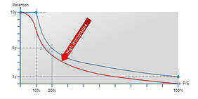
Image 4: While an SLC flash memory survives about 100,000 write/erase cycles, an MLC memory and a TLC memory only achieve roughly 3,000 and 500 write/erase cycles respectively. One PE cycle is only reached once the complete density, i.e. capacity, of the memory has been written.
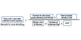
The number of possible write/erase cycles (PE cycles), the so-called endurance rate, decreases as the number of bits per cell increases. As a rule, the actual amount of written data differs from the data sent by the microprocessor. Due to the system optimization of the flash, 4 KB of sent data are, e.g., written several times within the NAND. To better estimate the effectiveness with which the data are transferred from the host to the memory, the amount of data can be quantified using the WAF.
The WAF thus also has a negative impact on the endurance, as, in some circumstances, significantly more data were written than were actually stored. This factor goes hand in hand with both wear leveling and garbage collection.
Image 5
So-called wear leveling ensures that each memory cell is used and deleted equally. The data retention, i.e. the maximum time span in which the data can still be retrieved in the data field after programming, thus increases and prolongs the longevity of a flash device. The more write/erase cycles an application has or the higher the average operating temperature is, the more likely it is to use MLC or even SLC flash memory in order to ensure a sufficient life span of the module.
An important instrument for ensuring the longevity of memories is the ECC - an error correction method that compares all the bits with the checksum when reading out the memory and thus identifies and corrects any faulty cells. The amount of errors that can be dictated depends on the size of the ECC (e.g. 8 bits). If the function is assumed by the host, it is essential to check the compatibility between the memory and the processor.
Older processors, in particular, have an integrated ECC that no longer supports newer memory models. However, in order to be able to support these customers in the future, Rutronik collaborates with two memory suppliers, INSIGNIS and Alliance Memory, which offer older and compatible derivatives. When using Toshiba Flash, it is also possible to apply BENAND™ as an alternative. This SLC NAND has an integrated ECC which assumes error correction directly in the memory, and the host has absolutely no influence on it.
If the microprocessor does not have a NAND interface (as is the case with RZ/A1L), conventional NOR flash or Serial NAND can be used. These memories have an SPI interface that is integrated as standard for microcontrollers and processors. Another variant is already managed NAND memories. Management is provided by a control unit integrated in the memory. The so-called e·MMCs (embedded multi media cards) are mostly manufactured in MLC technology. Functions such as bad block management, wear leveling, and garbage collection are also contained in the memory and do not have to be assumed by the host, i.e. the microprocessor.
Working memory for all requirements
If the RAM integrated in the host is insufficient, it can also be supplemented by an external memory. Internal RAM of between 3 and 10 MB is available for the RZ/A processors. The RZ/G series can be extended with external RAM. The volatile memory types SRAM (static RAM) and SDRAM (dynamic RAM) are available for external RAM. SRAM provides fast access and can preserve stored data for up to several years. However, SRAM only offers small data capacities, requires a lot of space on the PCB, and is much more expensive than DRAM. Although DRAM only offers average access times and needs a cyclical refresh for data preservation, it is characterized by high data density on a small surface at a favorable price.
SDRAM, in turn, is available as a SDR (single data rate) and a DDR (double data rate) model. Compared to SDR memories, DDR memories can transfer twice the data rate, since they use the rising and falling clock edges of the data signal for transmission. Prefetching is used to shorten the relatively slow access time of the SDRAM. The DDR memory accesses several memory cells in parallel. The data written in a buffer is then output at the higher external data rate of the host. While the original DDR technology works with double prefetching, DDR2 uses fourfold prefetching and DDR3 and DDR4 both use eightfold prefetching.
Both types of memory have advantages and disadvantages. A combination of all the advantages seems unrealistic but is actually possible with FRAM. FRAM (ferroelectric random access memory) uses its special technology to combine three important advantages: It is fast (150 ns access time) and ensures very low power consumption and a significantly longer lifetime than flash or SDRAM (10 million read/write cycles). In addition, FRAM - even if the name suggests otherwise - are non-volatile memories and therefore the data remain stored even in the event of power loss. However, Fujitsu offers only small capacities with its memory form - comparable with EEPROM – which can offer the perfect solution especially for metering/energy, point of sales, and IoT applications.
When it comes to choosing the right memory, it is, therefore, important to ask yourself the right questions: What do I want to store and for how long? What will the loss of data cost? Which endurance and data retention rate do I need to achieve my goals?
Once all these questions have been answered clearly, the result is perfect interaction between the MPU and the memory.
Glossary:
Bad block management = detection of defective data blocks
Buildroot = simple, efficient, and easy-to-use tool for creating embedded Linux systems
BSP = board support package
ECC = error correcting code
Garbage collection = automatic memory clean-up
GitHub = online service that provides software development projects on its servers
GPU = graphics processing unit
PCB= printed circuit board
Prefetching = pre-call of memory contents
RAM = random access memory
uboot = a universal boot loader
WAF = write amplification factor
Wear leveling = memory wear compensation